- 您现在的位置:买卖IC网 > Sheet目录323 > DSP56311EVM (Freescale Semiconductor)KIT EVALUATION FOR DSP56311
�� �
�
�Serial� Communication� Interface� (SCI)�
�The� SCI� clock� determines� the� data� transmission� (baud)� rate� and� can� also� establish� a� periodic�
�interrupt� that� can� act� as� an� event� timer� or� be� used� in� any� other� timing� function.� Bits� CD11–� CD0,�
�SCP,� and� SCR[STIR]� work� together� to� determine� the� time� base.� If� SCR[TMIE]� =� 1� when� the�
�periodic� time-out� occurs,� the� SCI� timer� interrupt� is� recognized� and� pending.� The� SCI� timer�
�interrupt� is� automatically� cleared� when� the� interrupt� is� serviced.� This� interrupt� occurs� every� time�
�the� periodic� timer� times� out.�
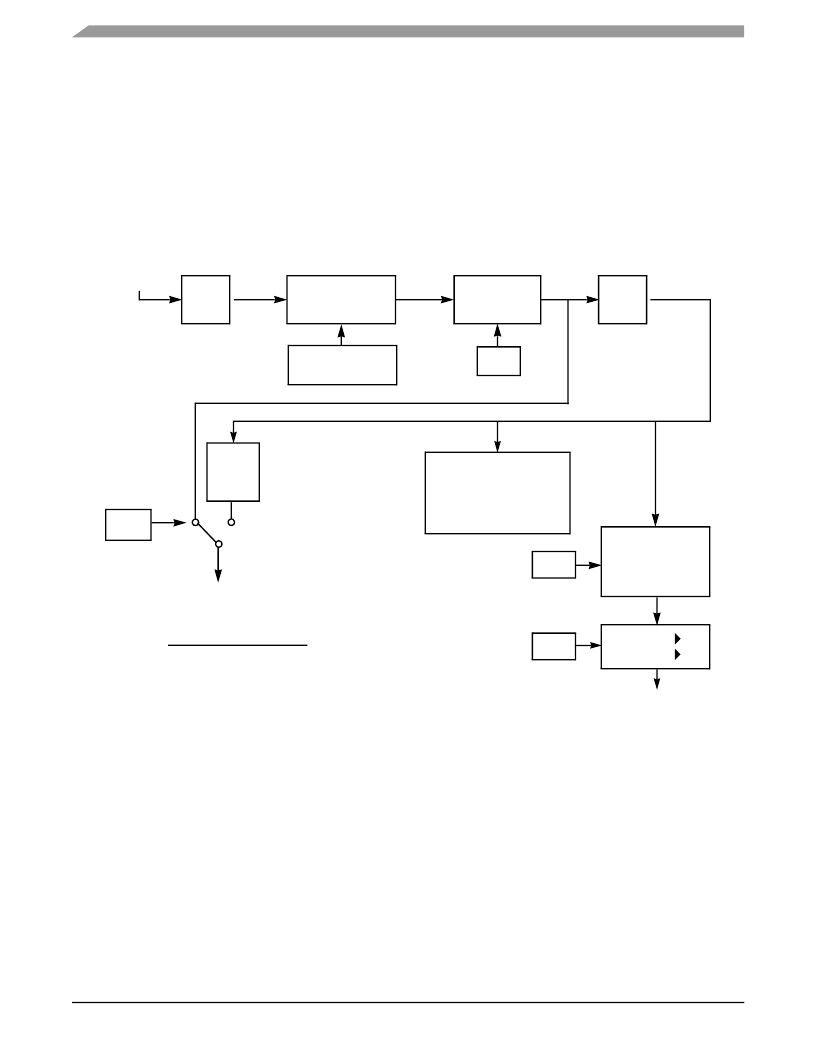
�Figure� 8-5� shows� the� block� diagram� of� the� internal� clock� generation� circuitry� with� the� formula� to�
�compute� the� bit� rate� when� the� internal� clock� is� used.�
�F� core�
�Divide�
�By� 2�
�12-bit� Counter�
�Prescaler:�
�Divide� by�
�1� or� 8�
�Divide�
�By� 2�
�STIR�
�Divide�
�by� 16�
�CD[11–0]�
�SCP�
�SCI� Core� Logic�
�Uses� Divide� by� 16� for�
�Asynchronous�
�Uses� Divide� by� 2� for�
�Synchronous�
�Internal� Clock�
�If� Asynchronous�
�Divide� by� 1� or� 16�
�Timer�
�Interrupt�
�(STMINT)�
�COD�
�If� Synchronous�
�Divide� By� 2�
�Fcore�
�bps� =� 64� � (7(SCP)� +� 1)� � CD� +� 1)�
�SCKP�
�SCKP� =� 0� +�
�SCKP� =� 1� -�
�where:� SCP� =� 0� or� 1�
�CD� =� $000� to� $FFF�
�SCLK�
�Figure� 8-5.� SCI� Baud� Rate� Generator�
�As� noted� in� Section� 8.6.1� ,� the� SCI� can� be� configured� to� operate� in� a� single� Synchronous� mode� or�
�one� of� five� Asynchronous� modes.� Synchronous� mode� requires� that� the� TX� and� RX� clocks� use� the�
�same� source,� but� that� source� may� be� the� internal� SCI� clock� if� the� SCI� is� configured� as� a� master�
�device� or� an� external� clock� if� the� SCI� is� configured� as� a� slave� device.� Asynchronous� modes� may�
�use� clocks� from� the� same� source� (internal� or� external)� or� different� sources� for� the� TX� clock� and�
�the� RX� clock.�
�For� synchronous� operation,� the� SCI� uses� a� clock� that� is� equal� to� the� two� times� the� desired� bit� rate�
�(designated� as� the� 2� � clock)� for� both� internal� and� external� clock� sources.� It� must� use� the� same�
�source� for� both� the� TX� and� RX� clock.� The� internal� clock� is� used� if� the� SCI� is� the� master� device�
�DSP56311� User’s� Manual,� Rev.� 2�
�8-18�
�Freescale� Semiconductor�
�发布紧急采购,3分钟左右您将得到回复。
相关PDF资料
DSPAUDIOEVMMB1E
BOARD MOTHER DSP563XX
DSPIC30F2010 DEVELOPMENT KIT
KIT DEV EMBEDDED C
DSTRM-KT-0181A
DSTREAM DEBUG AND TRACE UNIT
DSUT1CSU
SURGE SUPPR NETWORK W/GROUND
DTEL2
SURGE SUPPRESSOR PHONE RJ11/RJ45
DV003001
PROGRAMMER PICSTART PLUS 16C/17C
DV164035
MPLAB ICD3 IN-CIRC DEBUGGER
DV164039
KIT DEV PIC24FJ256DA210
相关代理商/技术参数
DSP56311EVMIG_D
制造商:未知厂家 制造商全称:未知厂家 功能描述:DSP56311EVMIG DSP56311EVM Sample Code
DSP56311EVMUM
制造商:未知厂家 制造商全称:未知厂家 功能描述:DSP56311 Evaluation Module Hardware Reference Manual
DSP56311FACT
制造商:未知厂家 制造商全称:未知厂家 功能描述:DSP56311 Higher performance programmable DSP for demanding voice and data applications
DSP56311UM
制造商:未知厂家 制造商全称:未知厂家 功能描述:DSP56311 24-Bit Digital Signal Processor Users Manual
DSP56311UMAD
制造商:未知厂家 制造商全称:未知厂家 功能描述:DSP56311 Users Manual Addendum
DSP56311VF150
功能描述:数字信号处理器和控制器 - DSP, DSC 150Mhz/300MMACS 150Mhz EFCOP RoHS:否 制造商:Microchip Technology 核心:dsPIC 数据总线宽度:16 bit 程序存储器大小:16 KB 数据 RAM 大小:2 KB 最大时钟频率:40 MHz 可编程输入/输出端数量:35 定时器数量:3 设备每秒兆指令数:50 MIPs 工作电源电压:3.3 V 最大工作温度:+ 85 C 封装 / 箱体:TQFP-44 安装风格:SMD/SMT
DSP56311VF150B1
功能描述:数字信号处理器和控制器 - DSP, DSC 24 BIT DSP
RoHS:否 制造商:Microchip Technology 核心:dsPIC 数据总线宽度:16 bit 程序存储器大小:16 KB 数据 RAM 大小:2 KB 最大时钟频率:40 MHz 可编程输入/输出端数量:35 定时器数量:3 设备每秒兆指令数:50 MIPs 工作电源电压:3.3 V 最大工作温度:+ 85 C 封装 / 箱体:TQFP-44 安装风格:SMD/SMT
DSP56311VF150R2
功能描述:数字信号处理器和控制器 - DSP, DSC 24 BIT DSP RoHS:否 制造商:Microchip Technology 核心:dsPIC 数据总线宽度:16 bit 程序存储器大小:16 KB 数据 RAM 大小:2 KB 最大时钟频率:40 MHz 可编程输入/输出端数量:35 定时器数量:3 设备每秒兆指令数:50 MIPs 工作电源电压:3.3 V 最大工作温度:+ 85 C 封装 / 箱体:TQFP-44 安装风格:SMD/SMT